Pcb Design Project Report
Before beginning a pcb project, the students first review an online tutorial to. It makes use of copper as a conductive material for the connections as the components are soldered.
I made a PCB Business Card! Files to make your own too

This software is used by the design engineers to create the electronic schematics and prints.
Pcb design project report. Introduction the present report has been prepared on the pcb design and fabrication. June 01, 2018 by m. Innovation system plus strive to provide best support to our scholars.
Start by logging in to easyeda , and create a new project: The department of electronics and telecommunication (etc) engineering of dbce in association with fiire (forum for innovation incubation research and entrepreneurship) conducted a one day faculty development program (fdp) on “pcb design and fabrication” on august 19, 2020. The schematic for the circuit is designed.
The goal of the project is to design and manufacture a reconfigurable obstetrics delivery bed that is easy to clean and maneuver, robust, This article explores the schematic design and basic features of a smart programmable wireless controller module i designed: 4 pcb fabrication as per design input.
Paper, the design of a pcb milling and drilling machine, where motor to control drill. All reports are prepared by highly qualified consultants and. We can modify the project capacity and project cost as per your requirement.
As the overall project progresses, this knowledge of cad pcb design will be crucial as custom pcbs will need to be fabricated for prototyping. We can provide you detailed project reports on the following topics. Vlsi, vhdl and pcb design a industrial training report submitted in partial fulfillment of the requirement of the degree of bachelor of technology in electronics and communication engineering by richa bharti (reg no.20130707) under the guidance of dr.sagar bose training head.
Up to 10% cash back the students will get a brief knowledge of pcb engineering ,design and development along with a realtime project included in it. Each project consists of a useful practical circuit that is demonstrated with a neatly fabricated pcb. The scope of the report includes assessing market.
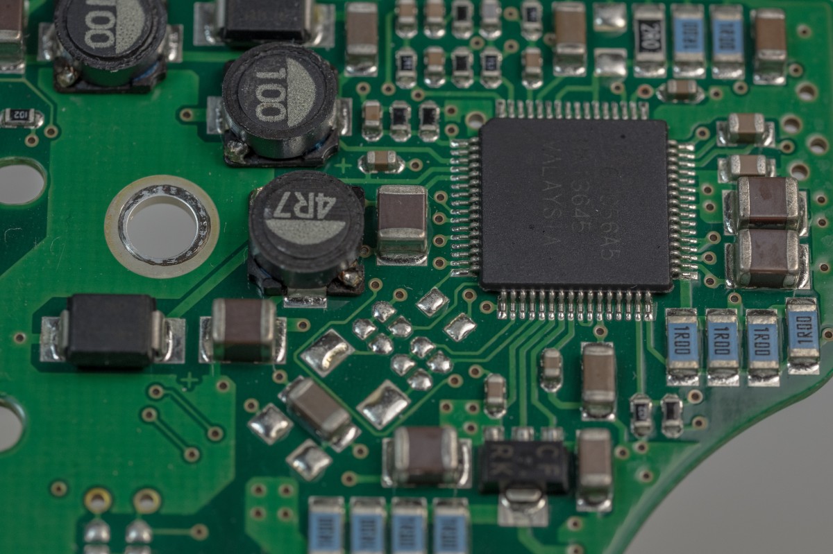
This report provides information obtained through ratio analysis. Printed circuit board (pcb) serves as a platform for organizing circuit components into a board. Connect the components according to the schematic.
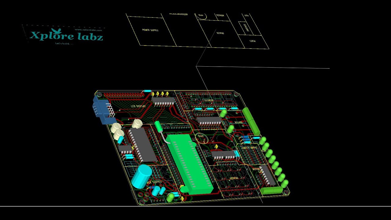
Completed pcb design of led flasher circuit. Thus due this the system is the drill holes and the layout are automatically find out from complicated and system becomes an image of the circuit in eagle software. This project also helps with the possibility of making a pcb for senior design.
This report details an engineering design project undertaken by mechanical engineering undergraduate students at the university of michigan. Detailed project report (dpr) on printed circuit board manufacturing plant (single, double & multilayer) present market position and expected future demand, technology, manufacturing process, investment opportunity, plant economics and project financials. Test a pcb for functionality.
Plus, the pcb editing software can import all of the components, footprints, and wires into the pcb file, which will make the design process easier (more on this later). Kanan how to stream sensor data from bosch’s xdk110 evaluation board to the mqtt messaging service First, ensure that an associated document (schematic or pcb) for the project that you wish to create the report for is the active document in the main design window.
The pcb is printed, fabricated, and assembled. Iit kanpur pcb design guide sheet page 10 of 26 exposure system after fixing layout‐films exactly on both sides of the laminated board the light sensitive cover is exposed by a ultraviolet light in double‐sided drawer exposure unit with a vacuum system. Comprehensive analysis from industry covering detailed reporting and evaluates the position of the industry by.
Using eda software, the board design is laid out. This report will pay particular attention to the training, and will management highlight major strength and weakness while. The pcb project was useful in learning about the basics of pcb design and layout.
Posted on december 7, 2016 by pam12004. Please select the projects of your interests. The students will be able to simulate the pcb into 3d and can view it and correct it for correction ,that is a unique.
The core objective of the. Each detailed project reports cover all the aspects of business, from analysing the market, confirming availability of various necessities such as plant & machinery, raw materials to forecasting the financial requirements. The students will get written material ,video lectures,pcb schematics ,designs for practice.
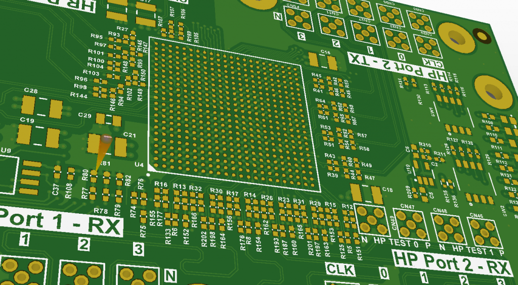
The below list provides you with a collection of diy pcb projects which can be used to develop pcb designing skills. Industrial training report of vlsi,vhdl and pcb designing 1. The design details including the gerber file.
Now select the “board edge” layer form the left bottom layer selecting drop down menu. After selecting the board edge layer, draw a rectangle around your pcb art work. This entry was posted in uncategorized by pam12004.
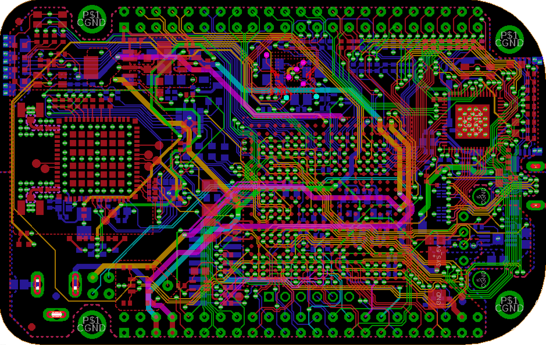
Project notes is the documentation center for your pcb design product. This paper focuses project does not use the path planning method. Pcb designing is a vital step in every product development cycle.
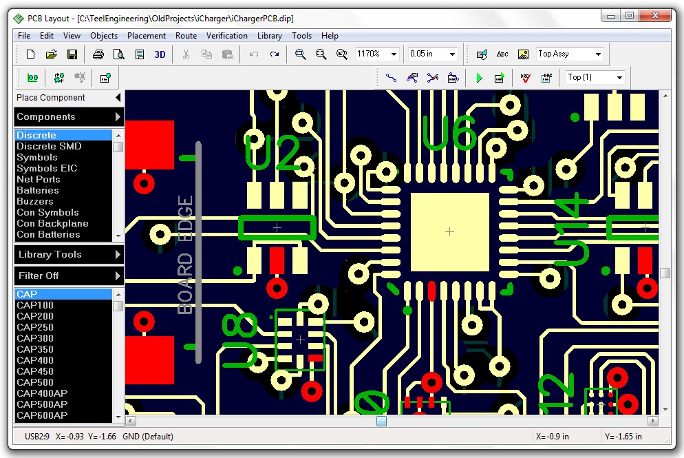
Report on pcb design and fabrication. It contains schematic capture editor, pcb layout editor, auto router, and bill of materials tools (bom). Easily applicable graphical layout editor or eagle is a solution driven pcb design program.
KiCad PCB Design for beginners = kickstarter YouTube
Free Images technology, gadget, developer, trace, lines
ECS Circuits Ireland's leading supplier of PCB PCB
PCB Layout Fast Forward DDR3 Memory Layout YouTube

I'm finishing pcb design for the plasma speaker, this is

PCB Bus Routing and Layout The Basics PCB Design Blog

Electronic Engineering Capabilities
With Software for RigidFlex Designing, You Can Define and
green seamless printed circuit board pattern Printed

PCB Design Software Which One is Best?
WiFi 6 PCB Design Guide and 802.11 Standards Blogs Altium

HomeAutomationPCB Share Project PCBWay

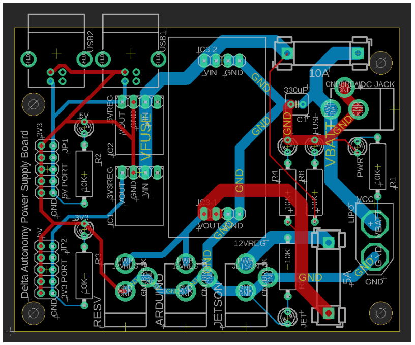
PCB Design Delta Autonomy
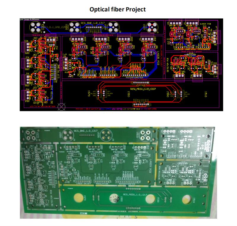
Some Good PCB Project Gerber Imgs For Share
Routing Differential Pairs in Altium Designer PCB Design

Worry Less About Schematic and Layout DeSync PCB Design
Should You Use Thick or Thin FR4 for Your PCB Substrate

Some Good PCB Project Gerber Imgs For Share

Learn Altium Essentials Doing PCB Layout (Lesson 4
